Analog to Digital Converter (ADC)
In order to interface analog sensors with your project, you will need to use the Analog to Digital Converter (ADC). The PIC16F690 has a 10-bit ADC. This means it provides readings from 0 to 1023 as the input voltage rises from Vss to Vref. Vref is the analog reference voltage and it can either be Vdd or supplied externally to the RA1/AN1/Vref pin.
In order to know the voltage applied at the analog input, the following formula is used:
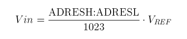 The formula for the input voltage from an ADC result.
The PIC16F690 has twelve analog input pins (AN0 through AN11). As discussed in the Digital I/O section, in order to enable the analog function for a pin, the corresponding bit must be set in the ANSEL or ANSELH register.
To explain the use of the ADC, let's look at a basic example taking a single reading.
#include <xc.h>
#pragma config FOSC=INTRCIO, WDTE=OFF, PWRTE=OFF, MCLRE=ON, CP=OFF, \
CPD=OFF, BOREN=OFF, IESO=OFF, FCMEN=OFF
#define _XTAL_FREQ 4000000
int main()
{
int result; //variable to store our ADC result
TRISA = 0xFF; //set all digital I/O to inputs
TRISB = 0xFF;
TRISC = 0xFF;
ANSEL = 0x00; //disable all analog ports
ANSELH = 0x00;
TRISAbits.TRISA2 = 1; //Disable the output driver for pin RA2/AN2
ANSELbits.ANS2 = 1; //set RA2/AN2 to analog mode
TRISBbits.TRISB7 = 0; //set RB7 as an output
///////////////
// ADC Setup //
///////////////
ADCON0bits.ADFM = 1; //ADC result is right justified
ADCON0bits.VCFG = 0; //Vdd is the +ve reference
ADCON1bits.ADCS = 0b001; //Fosc/8 is the conversion clock
//This is selected because the conversion
//clock period (Tad) must be greater than 1.5us.
//With a Fosc of 4MHz, Fosc/8 results in a Tad
//of 2us.
ADCON0bits.CHS = 2; //select analog input, AN2
ADCON0bits.ADON = 1; //Turn on the ADC
///////////////////////
// Main Program Loop //
///////////////////////
while(1)
{
__delay_us(5); //Wait the acquisition time (about 5us).
ADCON0bits.GO = 1; //start the conversion
while(ADCON0bits.GO==1){}; //wait for the conversion to end
result = (ADRESH<<8)+ADRESL; //combine the 10 bits of the conversion
if(result > 512)
PORTBbits.RB7 = 1; //turn on the LED if the input voltage is above Vdd/2
else
PORTBbits.RB7 = 0; //otherwise turn off the LED
}
return 0;
}
Let's go through the code.
ADCON0bits.ADFM = 1; //ADC result is right justified
First we determine how the ADC result is formatted. This is a 10-bit ADC and the result is stored in two registers, ADRESH and ADRESL. If we select right justification, the result will be stored like this:
| ADRESH | ADRESL |
| 7 | 6 | 5 | 4 | 3 | 2 | 1 | 0 | 7 | 6 | 5 | 4 | 3 | 2 | 1 | 0 |
| 0 | 0 | 0 | 0 | 0 | 0 | bit-9 | bit-8 | bit-7 | bit-6 | bit-5 | bit-4 | bit-3 | bit-2 | bit-1 | bit-0 |
This format allows us to store the result in an integer by simply shifting the ADRESH bits to the left by 8 and adding the ADRESL register: result = (ADRESH<<8)+ADRESL;
Selecting left justification results in the following:
| ADRESH | ADRESL |
| 7 | 6 | 5 | 4 | 3 | 2 | 1 | 0 | 7 | 6 | 5 | 4 | 3 | 2 | 1 | 0 |
| bit-9 | bit-8 | bit-7 | bit-6 | bit-5 | bit-4 | bit-3 | bit-2 | bit-1 | bit-0 | 0 | 0 | 0 | 0 | 0 | 0 |
This format is useful if you just want to use the 8 most significant bits of the result. In this case, you just simply copy the contens of the ADRESH register after the conversion is complete.
ADCON0bits.VCFG = 0; //Vdd is the +ve reference
Once we've selected our result format, we determine our voltage reference. By setting VCFG to 0, we are using the system positive supply (Vdd) as our reference. Writing a 1 to VCFG would allow us to use an external voltage reference connected to the RA1/AN1/VREF pin. External voltage references are used when a high level of accuracy is required. These can be ICs or zener diodes specially manufactured for voltage reference uses. Often these voltage references will have convenient values like 1.024V to make the volts/division an even number (1mV per division in this case).
ADCON1bits.ADCS = 0b001;
We then select our conversion clock source. The conversion clock must be selected so that the period is at least 1.5us (referred to as TAD in the datasheet). Since we are using a 4MHz clock, selecting Fosc/8 will provide a TAD of 2us (1/4,000,000 * 8 = 0.000002s = 2us). We could select Fosc/16, 32, or 64, but then the conversion would take longer than it has to.
ADCON0bits.CHS = 2;
Next we select which analog channel will be connected to the ADC. Since our sensor is connected to the AN2 pin, we write the number 2 to the CHS bits of the ADCON0 register.
ADCON0bits.ADON = 1;
Finally, we turn on the ADC.
while(1)
{
__delay_us(5); //Wait the acquisition time (about 5us).
ADCON0bits.GO = 1; //start the conversion
while(ADCON0bits.GO==1){}; //wait for the conversion to end
result = (ADRESH<<8)+ADRESL; //combine the 10 bits of the conversion
if(result > 512)
PORTBbits.RB7 = 1; //turn on the LED if the input voltage is above Vdd/2
else
PORTBbits.RB7 = 0; //otherwise turn off the LED
}
At this point, our program enters the program loop. At the beginning of each loop, there is a 5us delay. This is because it takes 5us for the analog sampling circuit to charge to the applied voltage (see datasheet section 9.3 for details). If we do not wait at least 5us, the reading will be lower than the actual voltage applied to the pin.
Once the acquisition time is passed, we start the conversion (ADCON0bits.GO = 1). While the ADC is working, the GO bit will remain HIGH. As soon as the ADC is done the conversion, the GO bit will be automatically reset. For this reason, the GO bit is polled in a while loop (while(ADCON0bits.GO==1){}). Once the bit returns to FALSE, the while loop condition fails and the program execution moves forward.
The conversion result is then saved in the variable 'result'. This is done by shifting the ADRESH register 8 bits to the left and then adding the ADRESL register. This results in a 16-bit integer from 0 to 1023.
Finally, the value of the result is checked. If the value is above 512 an LED is turned on and if it is below, it is turned off. Since 512 is the half way point, the LED will turn on any time the input voltage on the AN2 pin rises above Vdd/2. For example, if our circuit is 5V, the LED will turn on when the voltage at AN2 rises above 2.5V.
The voltage applied at the pin can also be calculated in software:
float voltage = (float)result/1023f*5.0f; //Assuming Vdd is 5.0V
The analog channel can be changed in between conversions by writing to the ADCS bits of the ADCON1 register. Just make sure you wait 5us before starting your conversion so the analog value is correctly sampled.
ADC Registers
Let's go through the ADC registers to see other options we have available.
| ADCON0 |
| 7 | 6 | 5 | 4 | 3 | 2 | 1 | 0 |
| ADFM | VCFG | CHS3 | CHS2 | CHS1 | CHS0 | GO/DONE | ADON |
ADFM: Analog result format. 0 = left justified (default), 1 = right justified.
VCFG: Voltage reference (VREF) selection. 0 = Vdd, 1 = VREF pin
CHS<3:0>: Analog channel select. This selects which voltage is fed into the ADC. Setting this anywhere from 0 to 11 selects AN0 to AN11 respectively. A setting of 12 feeds CVref (Comparator voltage reference). Setting CHS to 13 connects the 0.6V fixed voltage reference from the Comparator module to the ADC.
GO/DONE: Write a 1 to this bit to start an ADC conversion. Make sure to wait at least 5us before doing this after changing the input channel or performing a previous conversion. This bit is read to see if the current conversion is complete. The ADC will automatically reset this bit to 0 when conversion finishes.
ADON: ADC enable bit. 0 = ADC disabled and consumes no current, 1 = ADC enabled.
| ADCON1 |
| 7 | 6 | 5 | 4 | 3 | 2 | 1 | 0 |
| 0 | ADCS2 | ADCS1 | ADCS0 | 0 | 0 | 0 | 0 |
ADCS<2:0>: ADC clock select.
- 0b000 = Fosc/2
- 0b001 = Fosc/8
- 0b010 = Fosc/32
- 0b011 or 0b111 = FRC (internal oscillator)
- 0b100 = Fosc/4
- 0b101 = Fosc/16
- 0b110 = Fosc/64.
The bits marked as '0' are unimplemented and will always read as 0.
| PIE1 |
| 7 | 6 | 5 | 4 | 3 | 2 | 1 | 0 |
| 0 | ADIE | RCIE | TXIE | SSPIE | CCP1IE | TMR2IE | TMR1IE |
ADIE: ADC interrupt enable. Set this to 1 to generate interrupts when the ADC completes a conversion.
| PIR1 |
| 7 | 6 | 5 | 4 | 3 | 2 | 1 | 0 |
| 0 | ADIF | RCIF | TXIF | SSPIF | CCP1IF | TMR2IF | TMR1IF |
ADIF: ADC interrupt flag. This will be set to 1 by the ADC when a conversion completes. This must be cleared by software in the interrupt service routine to prepare the interrupt flag for the next conversion.
In order to use the ADC interrupts, the GIE (Global Interrupt Enable) and PEIE (Peripheral Interrupt Enable) bits in the INTCON register must be set to 1.
Using interrupts with the ADC can be beneficial so that the software does not have to sit idly polling the GO/DONE bit to determine when a conversion is complete.
This is the end of the Beginner's Guide. At this point you should be able to build any number of interesting projects! I hope you have found this information useful. For more advanced topics, you can look at the Intermediate Guide. However, I believe you should try to program some of your own projects before moving on.