Digital I/O
 Digital and analog pin diagram.
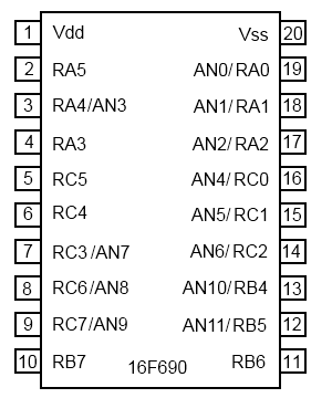
To the right is a pin diagram of the PIC16F690. You will notice that some pins have more than one name. That is because pins can serve more than one purpose and it is up to the designer to decide how each pin is configured.
ANSEL and ANSELH
There are several registers that affect the operation of the digital I/O pins. If you look at the pin diagram you will see that pin 3 is called RA4/AN3. This is because it can serve as digital I/O port RA4, or analog input pin AN3. The two registers ANSEL and ANSELH control whether or not AN0 through AN11 are operational. Each bit in the register controls one pin as outlined in the register tables shown below. A '0' sets the pin to digital mode and a '1' sets the pin to analog mode. For example, if you make ANSEL equal to 0b10000001 (binary), then AN7 will be enabled and RC3 will be disabled because they share the same pin (pin 7). AN0 will also be in analog mode (RA0 disabled). Reading a pin that is set to analog mode will return a '0'.
| ANSEL |
| 7 | 6 | 5 | 4 | 3 | 2 | 1 | 0 |
| ANS7 | ANS6 | ANS5 | ANS4 | ANS3 | ANS2 | ANS1 | ANS0 |
| ANSELH |
| 7 | 6 | 5 | 4 | 3 | 2 | 1 | 0 |
| X | X | X | X | ANS11 | ANS10 | ANS9 | ANS8 |
The code to set which pins are in analog mode will look something like the following:
ANSEL = 0b10000001; //AN7 and AN0 enabled
ANSELH = 0b00000101; //AN8 and AN10 enabled
Or we could use hex instead:
ANSEL = 0x81; //AN7 and AN0 enabled
ANSELH = 0x05; //AN8 and AN10 enabled
Because the 16F690 only has 12 analog inputs, you can write anything you want to the top 4 bits of ANSELH and it will have no effect. These are what the datasheet refer to as "unimplemented bits". I've shown my code writing 0s to those locations.
We can also access individual bits of a register. When you include xc.h at the beginning of your code, that file includes a header file for your device. In our case, it includes pic16f690.h. This file contains all the information for the registers in our device. It also contains unions for each register with each bit (or bit range) named. For example, there is a union called ANSELbits. In ANSELbits you will find ANS0, ANS1, ... , ANS7. Therefore, you can set an individual analog port as follows:
ANSELbits.ANS5 = 0; //disable AN5
TRISA, TRISB, and TRISC
The next set of registers to look at are the data direction registers. These registers, TRISA, TRISB, and TRISC control whether each digital I/O pin is an input or an output. The name TRIS is a shortening of tri-state which refers to the possible states of a pin: logic 1 output, logic 0 output, high-impedance input. Each bit in each TRIS register controls the data direction for one I/O pin. If the bit is set to 0, that pin is an output. If a bit is set to 1, that pin is an input. This is easy to remember because a 0 looks like an O for Output and a 1 looks like an I for Input.
| TRISA |
| 7 | 6 | 5 | 4 | 3 | 2 | 1 | 0 |
| X | X | TRISA5 | TRISA4 | TRISA3 | TRISA2 | TRISA1 | TRISA0 |
| TRISB |
| 7 | 6 | 5 | 4 | 3 | 2 | 1 | 0 |
| TRISB7 | TRISB6 | TRISB5 | TRISB4 | X | X | X | X |
| TRISC |
| 7 | 6 | 5 | 4 | 3 | 2 | 1 | 0 |
| TRISC7 | TRISC6 | TRISC5 | TRISC4 | TRISC3 | TRISC2 | TRISC1 | TRISC0 |
Once again, some bits are unimplemented because those pins do not exist on this device.
Code to set the data direction for the I/O pins might look as follows:
TRISA = 0b00110000; //RA5 and RA4 are digital inputs, the rest
//are outputs
TRISB = 0b10010000; //RB7 and RB4 are digital inputs, RB6 and RB5
//are outputs
TRISC = 0b00010001; //RC4 and RC0 are digital inputs, the rest
//are outputs
Note: Any analog pins must be disabled using the ANSEL and ANSELH registers before they can be used as digital I/O.
Note: Pin RA3, which is shared with MCLR, is an input only. Therefore, writing to bit 3 of TRISA will have no effect. Reading bit 3 will always return a 1, as RA3 is input only.
For example, if we wanted to use RC0 as a digital output pin we would first have to make sure the ANSEL bit for AN4 was disabled. This is necessary because it shares a pin with RC0.
ANSELbits.ANS4 = 0; //disable AN4
TRISCbits.TRISC0 = 0; //RC0 is a digital output
Once again, we can set or clear individual bits of the TRIS registers. The union in pic16f690.h is called TRISXbits where 'X' is A, B, or C. Each individual bit is called TRISX# where 'X' is A, B, or C, and # is the pin number. For example, to access the data direction bit for pin RA4 we would write to TRISAbits.TRISA4.
Note: It is a common mistake to set the ANSEL and ANSELH registers incorrectly or to forget to set them at all. If you are having trouble with a digital pin, check ANSEL and ANSELH.
Note: The bits of ANSEL and ANSELH default to '1' on power on. If you do not set these registers in your code, all the analog pins will be enabled. Therefore, no digital pins that share an analog pin will function correctly. Always set ANSEL and ANSELH.
PORTA, PORTB, and PORTC
Finally, the PORTA, PORTB, and PORTC registers hold the current digital state of the digital I/O. If you read these registers, you can determine which pins are currently HIGH or LOW. This is how you read a digital input. You can also read a digital output to check its current status.
Writing to the PORTX registers will set the digital output latches. Writing to a pin that is currently an input will have no effect on the pin because the output latch will be disabled.
| PORTA |
| 7 | 6 | 5 | 4 | 3 | 2 | 1 | 0 |
| X | X | RA5 | RA4 | RA3 | RA2 | RA1 | RA0 |
| PORTB |
| 7 | 6 | 5 | 4 | 3 | 2 | 1 | 0 |
| RB7 | RB6 | RB5 | RB4 | X | X | X | X |
| PORTC |
| 7 | 6 | 5 | 4 | 3 | 2 | 1 | 0 |
| RC7 | RC6 | RC5 | RC4 | RC3 | RC2 | RC1 | RC0 |
Here is an example of turning on digital output pin RB5:
ANSELHbits.ANS11 = 0; //disable AN11 shared with RB5
TRISBbits.TRISB5 = 0; //RB5 is a digital output
PORTBbits.RB5 = 1; //turn on the output
We can also set RB4 to be a digital input and read it:
ANSELHbits.ANS10 = 0; //disable AN10 shared with RB4
TRISBbits.TRISB4 = 1; //RB4 is a digital input
if(PORTBbits.RB4 == 1) //read RB4 and compare it to 1
PORTBbits.RB5 = 1; //if 1, turn on the output
else
PORTBbits.RB5 = 0; //if not, turn off the output
Hello World!
Now that we can configure our digital I/O, let's create the microcontroller version of "Hello World!".
For this example, connect an LED with a series resistor (220-470 Ohm) to pin 10 (RB7).
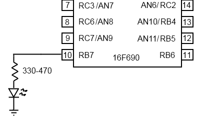 Adding the LED.
We will begin by disabling all analog inputs (because we aren't using any). We will then set all digital I/O pins to be inputs. After that we will individually set pin RC0 to be an output. Finally, we will enter an endless loop and make the LED blink.
The code to accomplish this is shown below. Replace the contents of your main.c file created in the MPLAB X & XC8 section of the guide. You can also directly download this code with comments here: main.c
#include <xc.h>
#define _XTAL_FREQ 4000000
#pragma config FOSC=INTRCIO, WDTE=OFF, PWRTE=OFF, MCLRE=ON, CP=OFF, \
CPD=OFF, BOREN=OFF, IESO=OFF, FCMEN=OFF
int main()
{
TRISA = 0xFF;
TRISB = 0xFF;
TRISC = 0xFF;
ANSEL = 0x00;
ANSELH = 0x00;
TRISBbits.TRISB7 = 0;
while(1)
{
PORTBbits.RB7 = 1;
__delay_ms(500);
PORTBbits.RB7 = 0;
__delay_ms(500);
}
return 0;
}
#pragma config is used to set the configuration bits of the microcontroller. In the PIC16F690 these are held in the register CONFIG. Some devices have more than one configuration register. We will cover the configuration settings later.
The __delay_ms() function is provided by XC8. It requires you define _XTAL_FREQ as the frequency of your system clock. We are using the internal oscillator at its default 4MHz, so _XTAL_FREQ is defined as 4000000. The compiler then uses that value to calculate how many cycles are required to give the requested delay. There is also __delay_us() for microseconds and _delay() to delay for a specific number of clock cycles. Note that __delay_ms() and __delay_us() begin with a double underscore whereas _delay() begins with a single underscore.
Note that the delay functions completely halt execution for their duration. During a delay the microcontroller performs a series of NOP() commands (NOP stands for No Operation and is essentially a "do nothing" command). If we want to do other things while we are waiting for a certain amount of time to expire, we will need to use timers. Those will be covered later.
It is good practice to use #define statements to provide logical names to pins. In the example above, we could include the following definition:
#define LED PORTBbits.RB7
#define LED_TRIS TRISBbits.TRISB7
Having done this, the code to make the LED blink would look like this:
LED_TRIS = 0; //Make the LED pin an output
while(1)
{
LED = 1; //Flash the LED
__delay_ms(500);
LED = 0;
__delay_ms(500);
}
Creating definitions for your pin names will go a long way towards making your code easier to understand. This will help you reduce errors and minimize the time you spend debugging.
In the next section we will learn about how interrupts are implemented. This will be useful for us as we learn how to use some of the peripheral features of the microcontroller such as timers.